Solutions for all of
your use cases.
μLEDs and
μLED Arrays
We provide your desired GaN solution – also for LEDs. No matter what size – the smaller the better. No matter what quantity. Precision guaranteed.
1...100 μm
290...1100 nm
A look at the
product
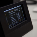
Qubedot’s μLEDs can be used as simple as any conventional LED. We designed a special driver electronic to control your μLED array. It comes with the software μ-controlLED to get you started directly with an easy-to-use GUI.
QubeDot´s µLEDs typically have a size of 1 … 100 µm and also a wavelength according to customers desires. Power densities of 150 kW/m² illuminate anything you put in the beam path. If you look at applications that need to run for many years, µLEDs are your solution as – for example – a µLED with a size of 5 µm draws less than 1 µA.
μLED Systems
One application of µLEDs is a pigtailed µLED with a wall plug efficiency that is more than 100 times better than any product we have seen before.
Pigtailed μLED as an example application
Boreholes fit to known widespread LED-systems
Microscopy
We develop and manufacture your desired digital high-tech microscopes – individual, simple, portable, multifunctional. Our microscopes prioritize user-friendly interfaces without compromising accuracy.
Curious about our Microscopy Solutions?
Foundry Service
We provide your desired GaN solution. You have a chip design or a customized epi stack design in your mind? There is not much time to achieve your goals? We make it happen.
turnaround
staff
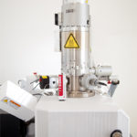
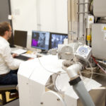
Semiconductor Analysis
Some people say “you can only manage what you can measure”. If you do not have the chance to manage your LED – or light related topic – we will gladly assist you with our experience and technical measuring equipment.
Among these are:
- Cathodoluminescence (CL)
- Time resolved cathodoluminescence (TR-CL)
- µPhotoluminescence (µ-PL)
- Energy-dispersive X-ray spectroscopy (EDX)
- Electrochemical Capacitance-Voltage (ECV)
- Time-of-Flight Mass Spectroscopy (TOF-MS)