Introducing our revolutionary microLED-platform SMILE


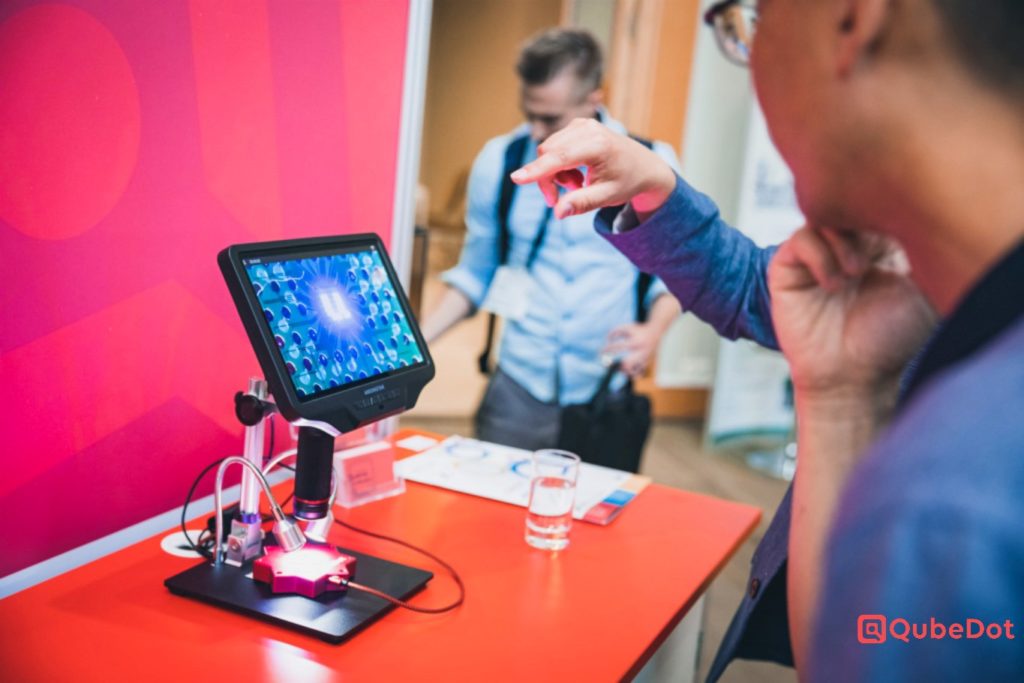
SMILE is an acronym for “Structured Micro Illumination Light Engine” and comprises our microLED-array in a ready-to-use format with different pixel numbers and sizes, wavelengths and intensities.
Our light sources are conveniently controlled directly from the computer via USB. The SMILE-platform includes a customized microLED chip, electronics, housing, and a graphical user interface for seamless control.


Our software enables the user to construct lighting patterns in a very convenient way. The graphical user interface provides the possibility of calibrating the array and adjusting the voltage. In addition, this interface allows the saving and loading of sequences and animations; and provides image and measurement windows for various use areas. An application programming interface allows the SMILE-platform control to be integrated into scrips and applications such as Matlab, LabView and Python.
 
SMILE-platform at a glance:
– Controllable light field 8 x 8 pixels of 75 µm size
– MicroLEDs individually controllable by software with up to 16 kHz
– Easy setup to create desired light patterns
– Robust housing, direct integration in optical path possible
– Ready for immediate use with GUI and USB cable
 
Are you interested in our SMILE platform? Contact us today to learn more.

Announcement: Forum MikroskopieTrends ’23

📢 Save the date – March 23, 2023!

We are very excited to announce that we are co-hosting the PhotonicNet “Forum MikroskopieTrends ’23” in cooperation with the Cluster of Excellence QuantumFrontiers.

The event will take place on March 23, 2023 at the Laboratory for Emerging Nanometrology LENA in Braunschweig.

Since 2001, the “Forum MikroskopieTrends” has been an established contact and discussion platform of the German microscopy scene with recognized high quality.

In addition to numerous professional presentations, our CEO Dr.-Ing. Heiko Brüning will talk about our customized microLEDs as an enabler for structured illumination and displays.

All details about the event and registration can be found here:
https://photonicnet.de/fileadmin/files/photonicnet/2023/Veranstaltungen/03/Forum_MikroskopieTrends_2023.pdf

The next generation of µLED technologies

As part of the EU project SMILE in which we are proud to be a project partner, a new generation of µLED technology is being developed.

Professor J. Daniel Prades from the Universitat de Barcelona visited the Quantum Valley Lower Saxony (QVLS) at the Mobile World Congress in Barcelona and gave this exciting interview:

https://magazin.tu-braunschweig.de/en/m-post/the-barcelona-braunschweig-led-connection/

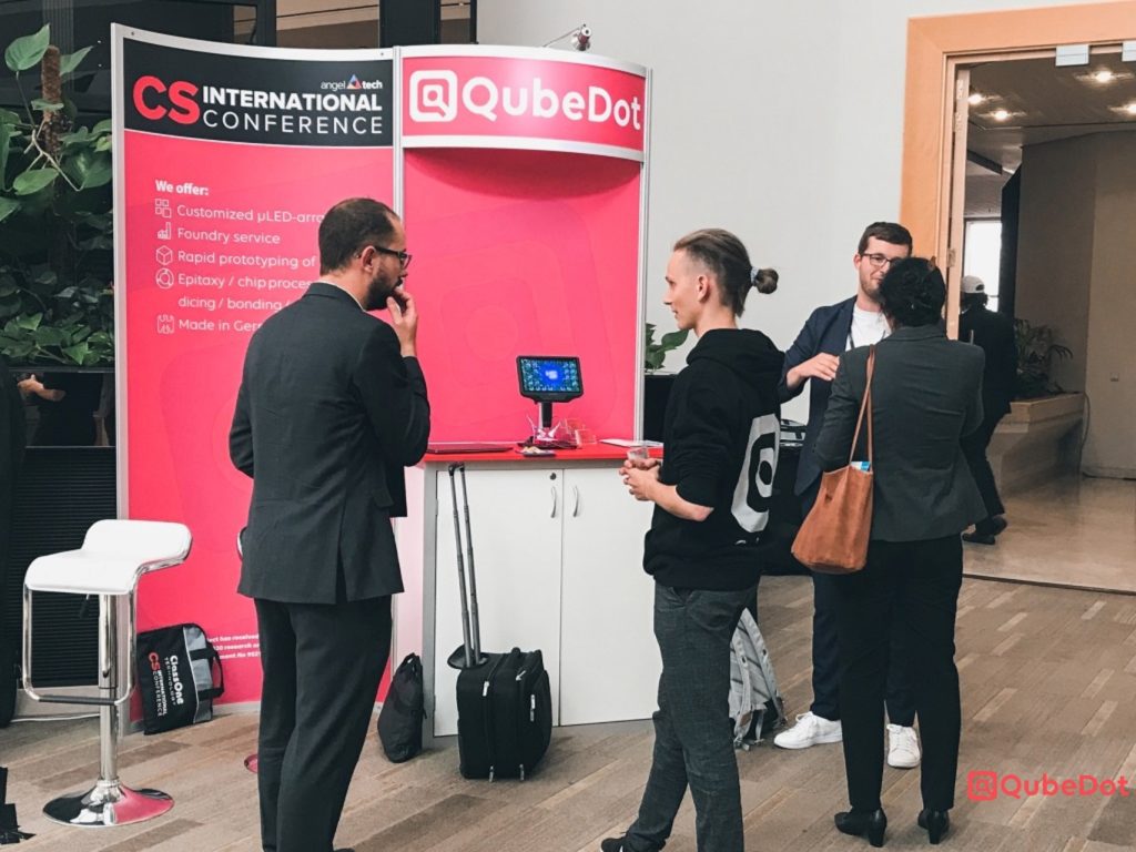
QubeDot at the CS International Conference in Brussels

Our team from QubeDot is very pleased to have been part of the CS International Conference in Brussels.

Jan, our CTO and Co-Founder of QubeDot, has given a talk about µLEDs for structured illumination and the versatility of our SMILE® Technology to address multiple markets.

µLEDs with dimensions of 1 to 50 µm are becoming increasingly interesting driven by the µLED revolution in display technology.

Our µLEDs are in addition also used – among other applications – in biology, optogenetics, microscopy and process metrology.

Do you want to know more about our customized µLEDs?

Here is the link to our solutions:

microLED-lines are very interesting

A glance at the portfolio of well-known suppliers of large, very powerful LEDs that emit on the order of several watts is enough to see that these LEDs are mostly round or square-shaped. But does that actually have to be the case? Doesn’t it make sense that LEDs could also be line-shaped for specific applications?

Some of our customers had also asked us this question. Of course, we don’t hesitate for long when it comes to such exciting questions. Our access to the clean room supports us in finding the appropriate answer within the shortest possible time. The answer to the question is “YES” – twice.

Yes, it can sometimes make sense to use linear microLEDs as well.

Yes, we can produce microLED lines.

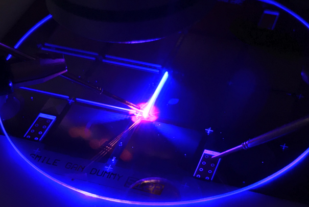
The picture shows a microLED line with a width of 10µm and a length of 1000µm. Of course, processed on GaN wafers – because that is our expertise!